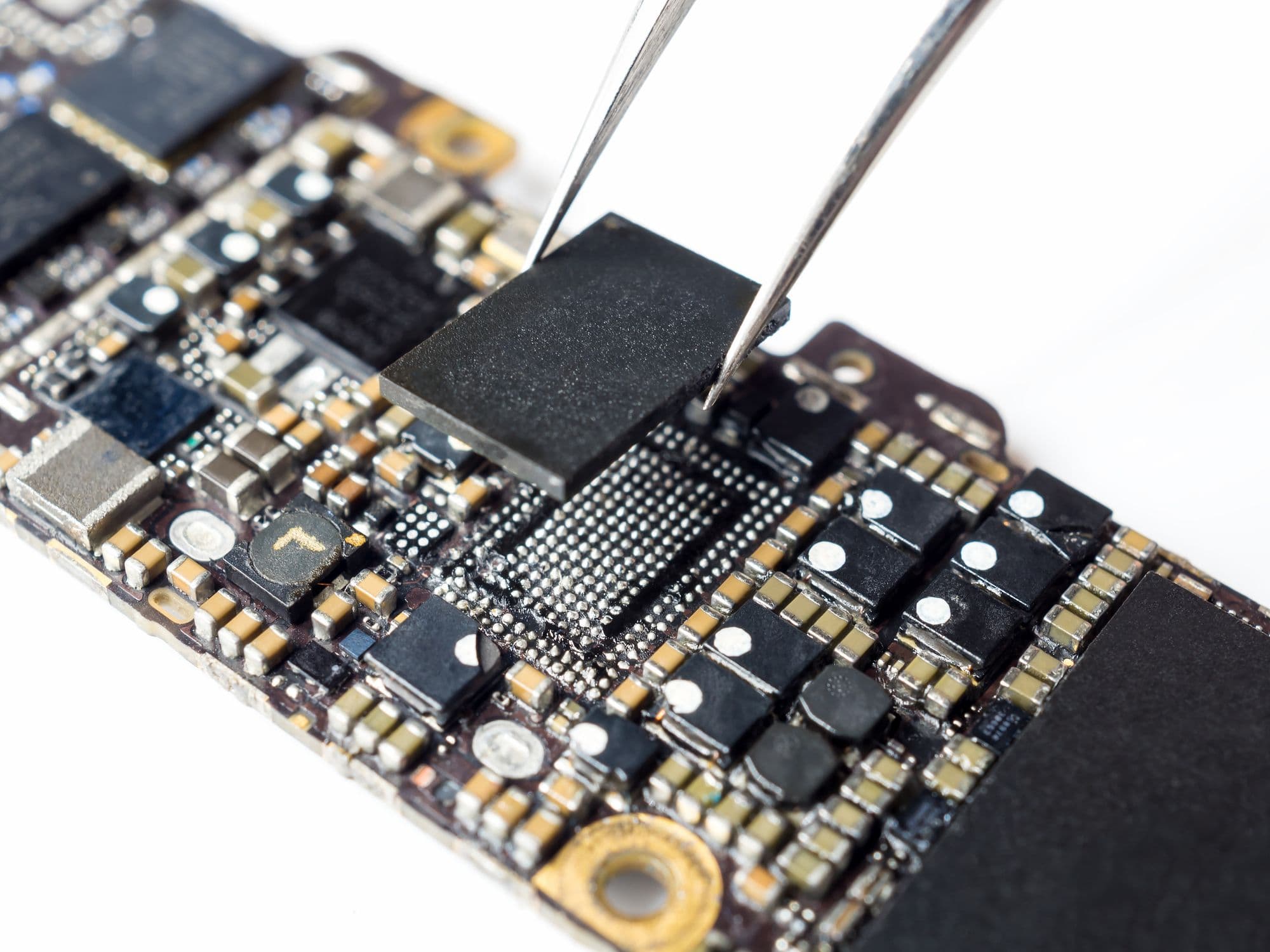
Dead-bugging — what is that, you ask? The concept comes from the idea that a memory chip, once it’s flipped over so you can attach wires to it, looks a little like a dead bug on its back.
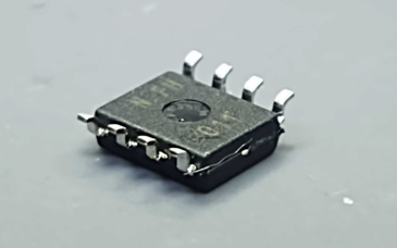
So why would we do this for the purposes of IoT hacking? The typical reason is if you want to extract the memory from the device, and you either don’t have a chip reader socket for that chip package type or your chip reader and socket pinouts don’t match the device.
I encounter this issue regularly with Ball Grid Array (BGA) memory devices. BGA devices don’t have legs like the chip shown above, but they do have small pads on the bottom, with small solder balls for attaching the device to a circuit board. The following BGA chip has 162 of these pads — here it is placed on a penny for size comparison.
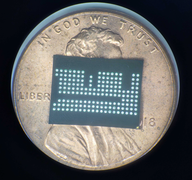
Sometimes, I encounter memory chips and don’t have a socket for attaching it to my chip reader. Sourcing the correct socket could take months, often from China, and I need to extract the data today. Other times, it’s just not cost-effective to purchase one of these sockets for my lab because I don’t encounter that chip package type very often. However, I do encounter the chip package type shown above all the time on embedded Multi Chip Packages (eMCP), and I have a chip reader for that device type.
Unfortunately, further research on this flash memory chip revealed that it is a Multi-Chip Package (MCP), meaning it does not have a built-in embedded controller, so my chip readers can’t interact with it. Also, I couldn’t find a chip reader socket that was even available to support this. This is where a little research and the dead-bugging method came in handy.
Getting started
The first step was to track down a datasheet for this Macronix memory chip MX63U1GC12HA. Once I located the datasheet, I searched it to identify key characteristics of the chip that I would help me match it to another chip package type, which I could target with my chip reader, an RT809H.
Although this MCP chip package has 162 pads on the bottom, most of those aren’t necessary for us to be able to access the flash memory. MCP packages contain both RAM and NAND Flash memory, so I only needed to find the pads associated with the NAND flash along with ground and power connection.
The next step I identified the correct chip type using the datasheet and identification number MX63U1GC12HA. Here’s what the components of that number mean:
- MX = Macronix
- 63 = NAND + LPDRAM
- U = NAND Voltage: 1.8V
- 1G = 1Gig NAND Density
- C = x8 Bus
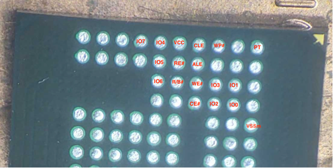
Next, the NAND flash pads I needed to identify and connect to were:
- I/O 0-7 = Data Input/Output x8
- CLE = Command Latch Enable
- ALE = Address Latch Enable
- CE# = Chip Enable
- WE# = Write Enable
- RE# = Read Enable
- WP# = Write Protect
- R/B# = Ready / Busy Out
- VCC = Voltage
- VSSm = Ground
- PT = Chip Protection Enable
With the datasheet, I also identified the above listed connection on the actual chip pad surface.
Typically, the hardest part is soldering the wires to these pads. This is the part that often scares most people away, but it looks harder than it really is. To avoid making it any harder than it has to be, I recommend going light on the coffee that morning – a recommendation I often don’t follow myself, which I end up regretting.
I have found one trick that works well to make attaching wires easier. This adds an extra step to the process but will speed things up later and remove much of the frustration. I recommend first attaching BGA balls to pads you need to attach wires to. Since the pads on this MCP chip are only 0.3 mm, I recommend using a microscope. I typically lay the balls by hand — once flux is placed on the chip surface, it’s simple to move the balls onto the pads one at a time and have them stay in place. Of course, this can also be done with solder paste and stencil. So, pick your favorite poison.
Once the balls have been placed on the correct pads, I place the chip in an InfraRed (IR) reflow oven to fix the balls to the pads. The lead-based BGA balls I use are Sn63/Pb37 and should melt at 183°C or 361°F. I use the following temperature curve set on my IR oven, which I determined using a thermal probe along with some trial-and-error methods. During the reflow process, it’s easy to accidentally damage a chip by overheating it, so take caution. My curve tops out just above 200°C, which has worked well, and I have yet to damage the chips using this curve.
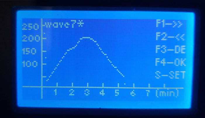
Once the oven has run through its cycle and the chip has cooled down, I clean the chip with alcohol to remove any remaining flux. If all goes well with the reballing process, the chip should have balls attached at each of the required locations, as shown below.
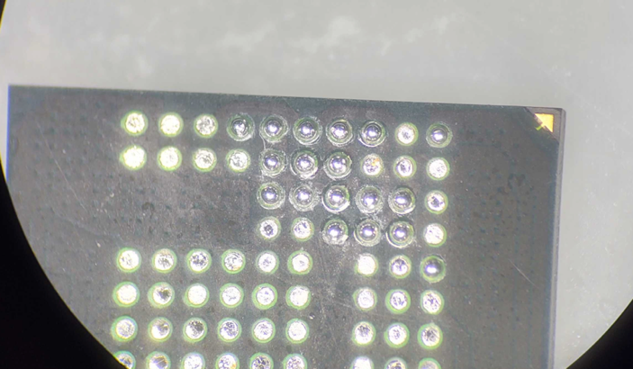
Attaching the wires
The next part is attaching wires to each of these pads. The wire I use for this is 40 gauge magnet wire, which is small enough to be attached to pads that are often .25 to .35 mm in size. This magnet wire is insulated with a thin coat of clear enamel, which can be problematic when soldering it to very small pads and trying to keeping the heat to a reasonable level. To resolve this issue, I burn the enamel insulation away and also coat the end of the wire with a thin coat of solder during that process. To do this, I melt solder onto the end of my solder iron and then stick the end of the magnet wire into the ball of solder on the end of the iron. This method works to remove the enamel insulation and tin the end of the wire, as shown below.
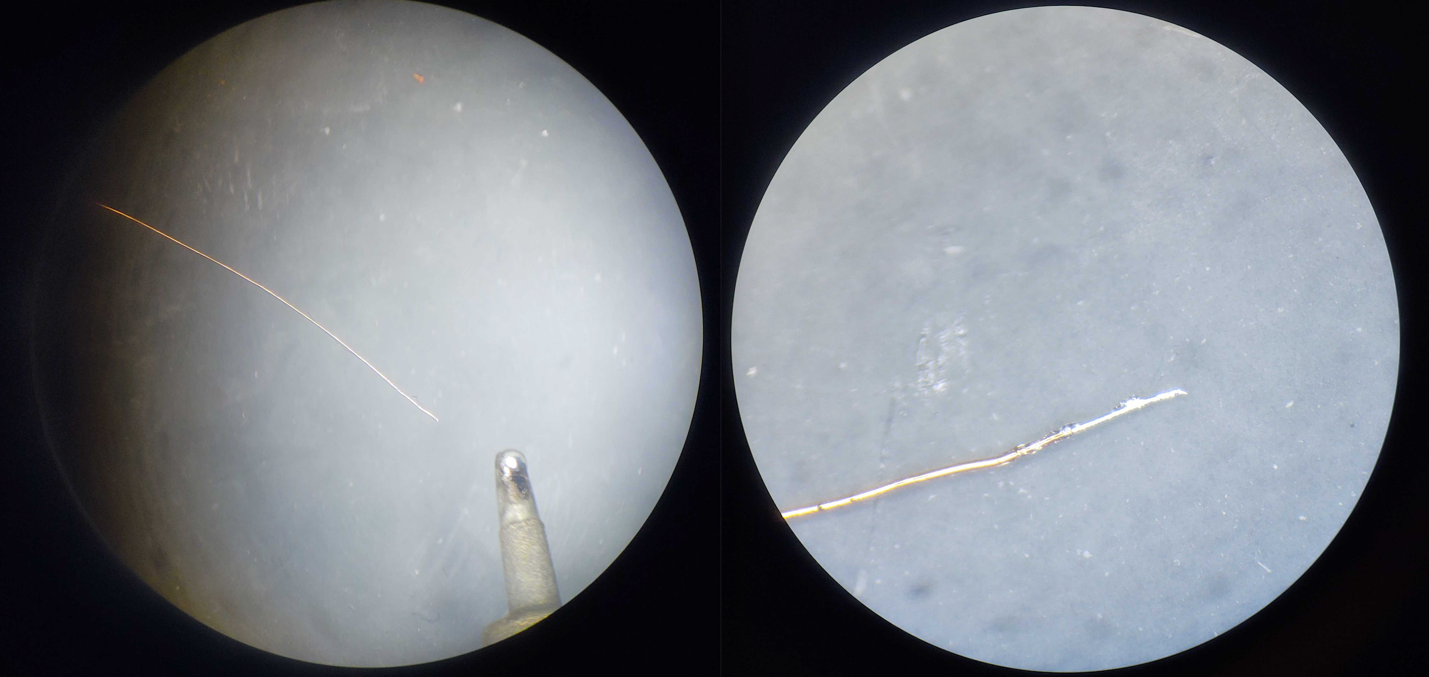
Once the magnet wire has been tinned, I next cut off the excess tinned area with wire cutters. How much you clip off depends on how big the pads are on the chip you’re attaching it to. The goal is to leave enough to properly solder it but not enough overhanging that could cause it to electrically short to other pads.

By pre-tinning the wire and adding solder balls to the chip pads, the process of attaching the wires becomes much quicker and less frustrating. To attach the wires, I take the tinned magnet wire and place a small amount of flux on the tinned area. Then, I push the wire against the solder ball on the chip pad I am attaching it to, and with the hot solder iron, I just barely touch the solder ball on the pad – instantly, the wire is attached. I use a micro-tip solder iron and set the heat high, so it is instant when I do this process. An example of this is shown below:
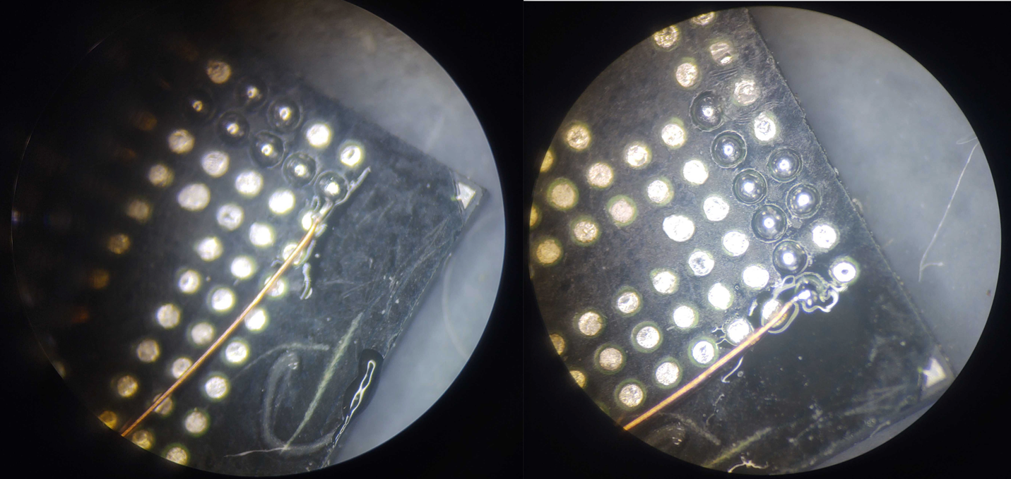
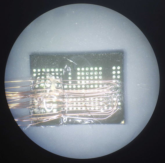
For the MX63U1GC12HA MCP chip, I used this process to attach all 17 of the needed wires, as shown below, and then held them in place using E6000 brand glue to prevent accidentally knocking the wires loose from mechanical stress on the solder joints.
Reading the chip
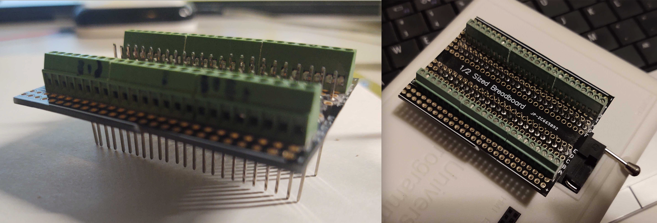
Next, it’s time to figure out how to read this chip to extract the firmware data from it. First, we need to attach the 17 wires to the chip reader. To do this, I custom-built a 48-pin Zero insertion force (ZIF) plug with screw terminals that I could attach to the ZIF socket of my RT809H chip programmer. This jig allows each wire to be attached via the screw terminals to any of the 48 pins as needed.
How we wire up a dead-bugged memory chip for reading depends on several things.
- Do we have a datasheet?
- Does the chip we are dead-bugging come in other package styles?
- Does the chip reader support the chip we have, and we just don’t have the correct socket?
- Does the manufacturer of our chip produce an unrelated chip that has a similar memory size, bus width, and layout?
Since I didn’t have a chip reader that supports this 162 BGA MCP device, I started looking for another Macronix chip that:
- Had 48 pins or less so I could wire it up to my chip reader
- Was a NAND Single Level Cell (SLC)
- Had 1g in density
- Had 8 bit bus
- Had operational voltage of 1.8v
After a little time Googling followed by digging through several different datasheets, I found a MX30UF1G18AC-TI, which was for a 48 TSOP package and appeared to match the key areas I was looking for.
Here’s what the name MX30UF1G18AC-TI tells us:
- MX = Macronix
- 30 = NAND
- U = 1.7V to 1.95V
- F = SLC
- 1G= 1G-bit
- 18A= 4-bit ECC with standard feature, x8
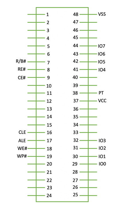
The diagrams found in the MX30UF1G18AC datasheet showed the pinout for the TSOP48 NAND memory chip. Using that data, I was able to match each of the required pins to the 162 BGA MCP MX63U1GC12HA so I could correctly wire each connection to the 48-pin ZIF socket for my RT809H chip programmer.
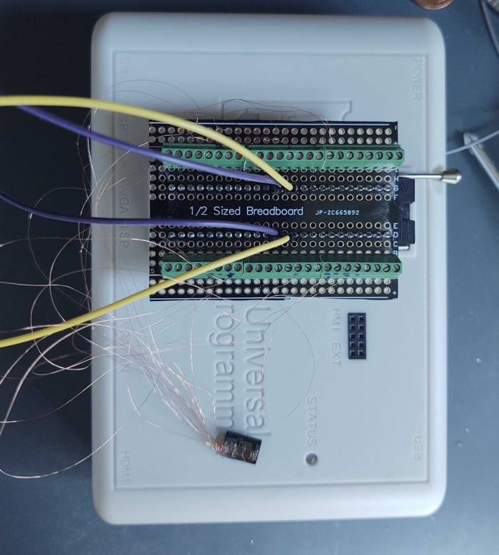
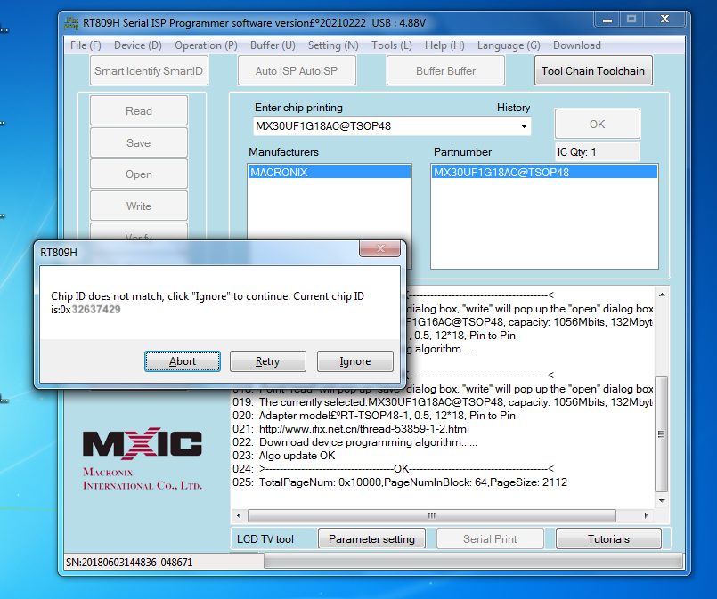
Once all of the connecting wires were properly connected to the screw terminal of my Zif socket, I selected the MX30UF1G18AC chip from the drop-down on the chip programmer and clicked “read.” As expected, the chip programmer first queried the chip for its ID. If it does not match, it will prompt you with “Chip ID does not match,” as shown below.
In this case, I selected “Ignore,” and the devices successfully extracted the data from the NAND flash chip. Some chip readers allow you to just turn this off before attempting to read the chip. Also, if the chip you’re reading is only different in package style, the chip ID will probably match.
The perfect solution is always to have all the proper equipment needed to read all memory chips you encounter, but very few pockets are that deep — or maybe the correct socket is months out for delivery, and you need the data from the chip today. In those cases, having the skills to do this work is important.
I have successfully used this process in a pinch many times to extract firmware from chips when I didn't have the proper sockets at hand – and in some cases, I didn’t have full datasheets either. If you have not done this, I recommend giving it a try. Expand those soldering skills, and build out test platforms and methods to further simplify the process. Eventually, you may need to use this method, and it’s always better to be prepared.
NEVER MISS A BLOG
Get the latest stories, expertise, and news about security today.
Subscribe